
Siemens Healthineers plans to build a new factory for cultivating crystals used in advanced computed tomography (CT) scanners.[Rendering courtesy of Siemens Healthineers]
Siemens Healthineers announced plans this week to build a factory in Germany for cultivating crystals used to make semiconductors for advanced computed tomography (CT) scanners.
The medtech giant said its existing production facility in Japan is at capacity, and that the new fabrication plant (or “fab”) is scheduled to come online in 2026.
Previously: FDA updates medical device shortage list due to shipping delays and semiconductors
The 9,000-m² Forchheim fab will cost 80 million euros, Seimens said. The company has invested around half a billion euros in its Forcheim operations since 2019.
“We made a conscious decision in favor of the Forchheim site. Here we are building the world’s first photon-counting CT scanner, Naeotom Alpha, whose demand has increased enormously since its market launch in 2021 due to its high-resolution imaging,” André Hartung, head of Siemens Healthineers diagnostic imaging, said in a news release. “In addition to a very good infrastructure, the region also offers many incentives for skilled workers.”
The new factory is expected to have around 100 employees.
Siemens Healthineers is the third-largest medical device in the world, according to Medical Design & Outsourcing‘s 2022 Medtech Big 100 ranking by revenue.
Related: 5 steps to help medical device makers deal with semiconductor shortages
Semiconductor crystals for sharper CT scans
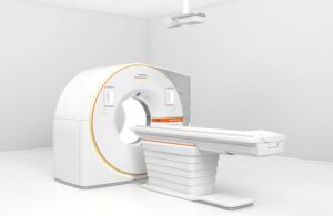
Siemens Healthineers’ Naeotom Alpha CT scanner [Image courtesy of Siemens Healthineers]
Siemens Healthineers uses the crystals as detector material for its newest photon-counting CT scanners to produce sharper images with a reduced dose of X-ray radiation. The new Naeotom Alpha CT scanner’s photon-counting detector’s detection layer consists of a cadmium telluride single crystal (CdTe). Siemens Healthineers said that offers advantages over conventional CT detectors.
“Conventional CT detectors first convert the X-rays into visible light in a two-stage process, which is then detected by a light sensor and generates the final image,” Siemens Healthineers explained. “As a result of this intermediate step, important information about the energy of the X-rays is lost and is no longer available to support the diagnosis: the contrast is reduced and the images become blurred. The photon-counting CT detector developed by Siemens Healthineers converts the X-ray photons directly into fully digital electrical signals. The image data offers new clinically relevant information and improved image resolution while at the same time reducing radiation dose.”
The FDA cleared the Naeotom Alpha in 2021, calling it “the first major new technology for computed tomography imaging in nearly a decade.”
Sustainable design at the Siemens Healthineers semiconductor facility
The new Forchheim facility is designed to achieve LEED Platinum certification for environmental sustainability. The company said the factory will be CO2 neutral, which means its operation will not emit greenhouse gasses that are contributing to global warming and climate change.
The building will use energy-efficient LED lighting and generate its own electricity with a 170kWp photovoltaic system on the roof. The building’s HVAC system will use waste heat from production to heat the buildings when needed, while shade from plants, bright-sealed surgaces and outdoor design features will keep the facility cool and prevent heat island effects.
The landscaping will include site-appropriate native species to promote local biodiversity. The outdoor lighting is designed to reduce light pollution for the benefit of nocturnal animals.